NANO PRO 4 inch Undoped 3C-SiC Epitaxial Wafer on Silicon, Epi Thickness: 300nm

SKU:
WA3001
SHIPPING:
Piece
IF YOU ARE INTERESTED IN A QUOTE FOR A LARGE QUANTITY, PLEASE CONTACT US
Email: Marknanossr@gmail.com
or
Get A Quotation

NANO PRO 4 inch Undoped 3C-SiC Epitaxial Wafer on Silicon, Epi Thickness: 300nm

Piece 1
Request a quotation.

Contact Us

Global Head Office

Email: Marknanossr@gmail.com

Tel:+86 15606950920

Wechat: 15606950920

Address:  Building 1, No. 39 Xinchang Road, Haicang District, Xiamen City, Fujian Province, China

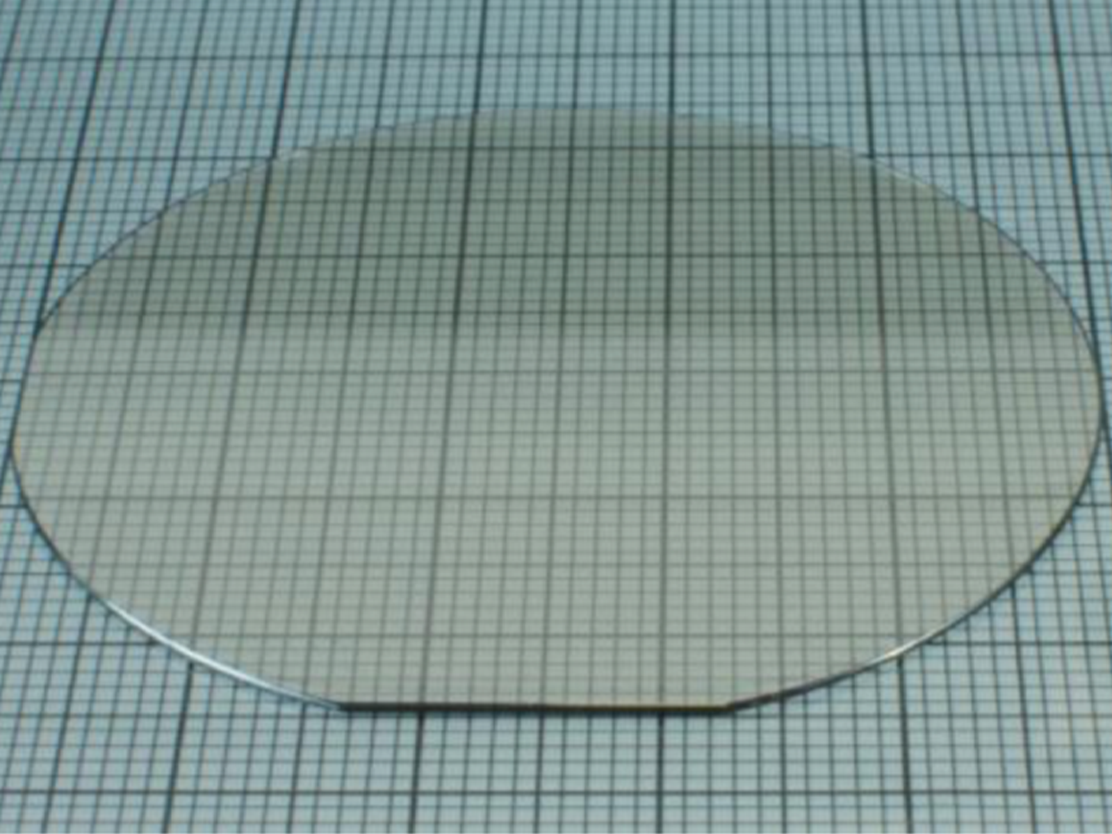
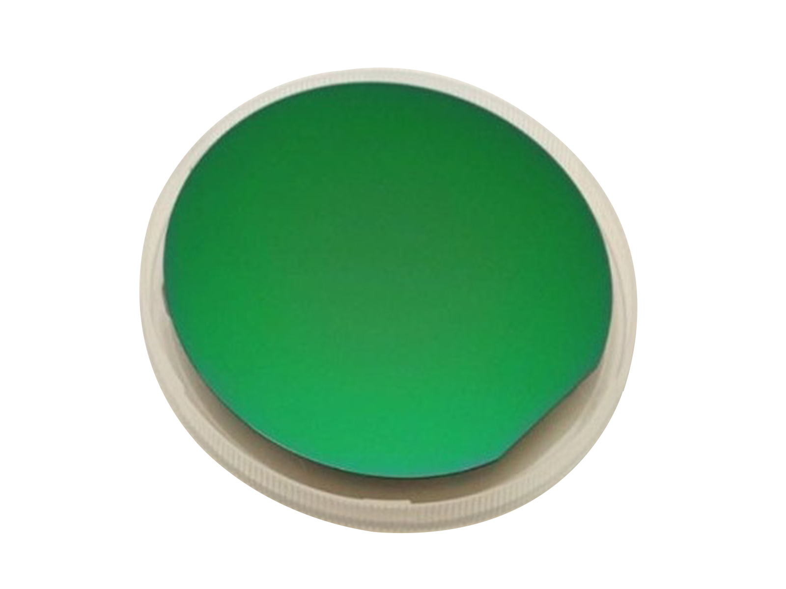
NANO PRO™ 4 inch Undoped 3C-SiC Epitaxial Wafer on Silicon, Epi Thickness: 300nm

3C-SiC belongs to the wide band gap semiconductor. Despite different polytypes, it has similar superior properties over traditional materials. It offers high resistance and semi insulating properties. During epitaxial growth, high concentration of electrically active dopants can be introduced into the 3C-SiC epitaxial layers, which helps avoid unnecessary ion implantation steps in device fabrication. The advantages of such wafer are reduced thermal stresses, compatibility with silicon technology, and comparable low cost. One of the applications of this epitaxial wafer is acting as the template for Gallium Nitride (GaN) growth, including hexagonal GaN and cubic GaN. The SiC layer on the silicon substrate can reduced the lattice spacing to about 4% mismatch to GaN (typically 17% for silicon and 14% for sapphire), which results in fewer crystal defects and further increases the performance of the devices. Since 3C-SiC is able to withstand high temperatures and corrosive chemicals, it is often used as a sensing devices that can operate in harsh environment. It can also be used for electronics, biomedical and clean energy applications.

NANOSSR offers epitaxy services on various substrate. Please contact us if you need customization or bulk order. 

SKU# WA3001

Specification:

Substrate Silicon Wafer
Diameter 100±0.2 mm
Grade Prime
Growth Method  CZ
Orientation  
Thickness 525±25 um
Resistivity  1~100 ohm.cm
Type/Dopant P-type/Boron
Epi Layer  3C-SiC
Epi Layer Thickness 300±30 nm
Epi Layer Type Undoped

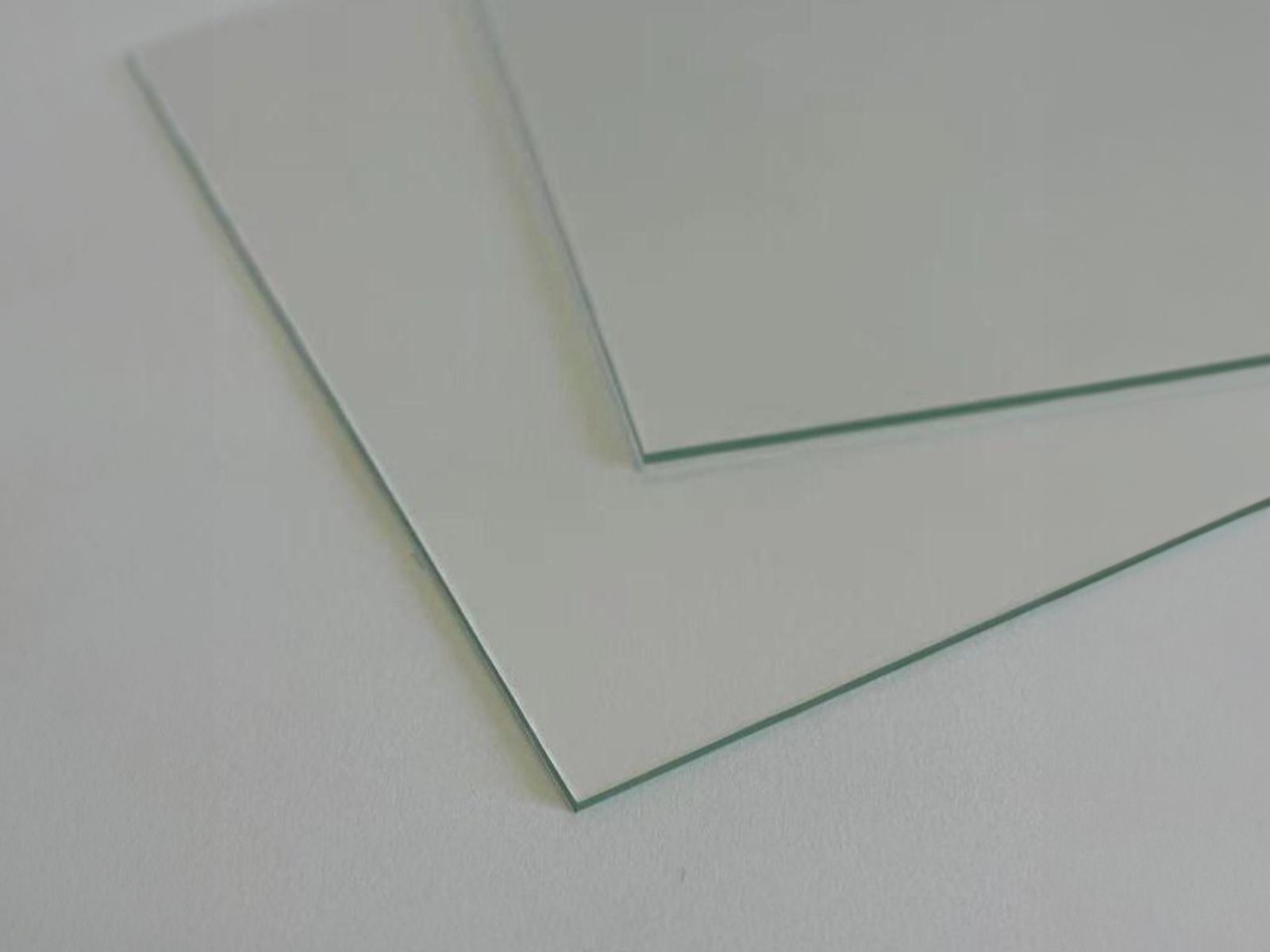
*Please note that actual products might be different from the picture below.

References:

1. 3C-SiC hetero-epitaxial growth on undulant Si (001) substrate. Journal of Crystal Growth 237 (2002): 1244-1249. 

2. 3C-SiC on Si hetero-epitaxial growth for electronic and biomedical applications. ECS Transactions 58, no. 4 (2013): 119.

3. 3C-SiC on Si: a versatile material for electronic, biomedical and clean energy applications. MRS Online Proceedings Library (OPL) 1693 (2014).

Customization:

NANOSSR offers 3C-SiC epitaxy services on various substrate as well, including SOI wafer and patterned substrate. We can also provide 4H-SiC homoepitaxial wafers. Please contact us if you need customized specification.

€ 4.00
GRAPHENE SHEET
Recent Posts

Future Communication with 5G Technology and Advanced Materials

Preserving History with the Power of Graphene
Future Communication with 5G Technology and Advanced Materials 5G technology opens the doors to a new era in communication with faster connection speeds, low late...

5G technology opens the doors to a new era in communication with faster connection speeds, low latency and wide coverage. This new generation technology enables important applications in many sectors...

​Graphite Applications on Anti-friction Coatings

Preserving History with the Power of Graphene
​Graphite Applications on Anti-friction Coatings Graphite is said to be known as one of the forms of carbon present in usually crystalline form. Thi...

Graphite is said to be known as one of the forms of carbon present in usually crystalline form. This too has various types and varieties in which graphite can be exhibited. However, recently it has c...

Cuprous (Copper) Oxide Properties and Applications

Preserving History with the Power of Graphene
Cuprous (Copper) Oxide Properties and Applications Cuprous oxide is also commonly known as copper oxide which is basically an inorganic compound compr...

Cuprous oxide is also commonly known as copper oxide which is basically an inorganic compound comprising of copper and oxygen. It has some excellent properties that enable it to surpass a lot of copp...

Cellulose Nanocrystals (CNC), Applications and Properties

Preserving History with the Power of Graphene
Cellulose Nanocrystals (CNC), Applications and Properties Cellulose is a very abundant polymer naturally available as it is a vital component present in vari...

Cellulose is a very abundant polymer naturally available as it is a vital component present in various plant cell walls. Besides, cellulose nanocrystals (CNC) also found in every other species all of...

Ketjen Black Applications As a Superconductor

Preserving History with the Power of Graphene
Ketjen Black Applications As a Superconductor Ketjen black is basically a conductive agent and conductive agents are usually used to make sure th...

Ketjen black is basically a conductive agent and conductive agents are usually used to make sure that the electrode possesses good charge and discharge performance. So ketjen black is responsible for...

​7 Reasons to Why Fullerenes are Growing Market

Preserving History with the Power of Graphene
​7 Reasons to Why Fullerenes are Growing Market Fullerene is a carbon allotrope consist of carbon atoms attached via single or double bonds.These m...

Fullerene is a carbon allotrope consist of carbon atoms attached via single or double bonds.These molecules have rich characteristics and potentially strong properties which enable them to work effec...

Molybdenum Disulfide (MoS2) Properties and Applications

Preserving History with the Power of Graphene
Molybdenum Disulfide (MoS2) Properties and Applications Molybdenum disulfide, also known as MoS2, is one of the best materials initially belonging to the t...

Molybdenum disulfide, also known as MoS2, is one of the best materials initially belonging to the transition metals.Its structure is unique hence all the properties it possesses are unique.  The buil...

From Graphene to the New Teflon

Preserving History with the Power of Graphene
From Graphene to the New Teflon Graphene is one of the most used materials in today's world and with all the exceptions that it is ...

Graphene is one of the most used materials in today's world and with all the exceptions that it is being used, it is being proven as one of the best materials for almost all industries.  Ever since i...

​Use of Graphene In The Textile Industry, Examples From The Market And Its Future

Preserving History with the Power of Graphene
​Use of Graphene In The Textile Industry, Examples From The Market And Its Future Graphene is known as a carbon allotrope in the industry as it comprises carbon atoms that are put t...

Graphene is known as a carbon allotrope in the industry as it comprises carbon atoms that are put together in the form of a lattice. Graphene is a highly necessary product in today's world as it is s...

IR Coating Technology and Applications

Preserving History with the Power of Graphene
IR Coating Technology and Applications IR coating technology is used for the optical coatings that perform their functions at a very large...

IR coating technology is used for the optical coatings that perform their functions at a very large scale. This includes UV wavelengths which are both short and long too. A lot of comprehensive studi...

Silicon Dioxide in Battery Applications

Preserving History with the Power of Graphene
Silicon Dioxide in Battery Applications Silicon dioxide is a promising material for next generation battery technologies because of its hig...

Silicon dioxide is a promising material for next generation battery technologies because of its high capacity and abundance. Especially Li-ion and Li-S batteries benefit from silicon dioxide and its ...

Properties of ​Ketjen Black as a Superconductor

Preserving History with the Power of Graphene
Properties of ​Ketjen Black as a Superconductor Ketjen black is basically a conductive agent and conductive agents are usually used to make sure th...

Ketjen black is basically a conductive agent and conductive agents are usually used to make sure that the electrode possesses good charge and discharge performance. So ketjen black is responsible for...

MoS2 Applications on Anti-friction Coatings

Preserving History with the Power of Graphene
MoS2 Applications on Anti-friction Coatings MoS2 is basically the chemical formula of molybdenum disulfide which is a compound known to be a tr...

MoS2 is basically the chemical formula of molybdenum disulfide which is a compound known to be a transition metal dichalcogenide having a blackish and silvery appearance. MoS2 is one of the categori...

​How to Sustainably Produce Nano Clays

Preserving History with the Power of Graphene
​How to Sustainably Produce Nano Clays Nanoclays, with their unique layered structure and nanometric size, are transforming industries by ...

Nanoclays, with their unique layered structure and nanometric size, are transforming industries by enhancing the performance of materials in packaging, automotive, and environmental engineering.  Th...

​10 Uses of Calcium Oxide in Daily Life

Preserving History with the Power of Graphene
​10 Uses of Calcium Oxide in Daily Life Calcium oxide is the chemical combination of calcium and oxygen subsequently forming a product that...

Calcium oxide is the chemical combination of calcium and oxygen subsequently forming a product that is rich in its characteristics and has an excellent set of properties that enable it to perform var...

​Cubic Boron Nitride Nanopowders: The New Diamond, Properties, and Applications

Preserving History with the Power of Graphene
​Cubic Boron Nitride Nanopowders: The New Diamond, Properties, and Applications Boron nitride is a chemical compound consisting of nitrogen and boron, having the chemical formula ...

Boron nitride is a chemical compound consisting of nitrogen and boron, having the chemical formula BN. It has various forms but the most common one is the cubic boron nitride form. It is actually a t...